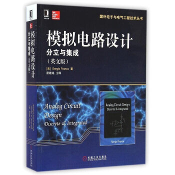
模拟电路设计:分立与集成(英文版) / 国外电子与电气工程技术丛书
¥119.00定价
作者: [美]Sergio Franco;雷鑑铭译
出版时间:2015-01
出版社:机械工业出版社
- 机械工业出版社
- 9787111489320
- 1版
- 319069
- 44217478-5
- 平装
- 16开
- 2015-01
- 1289
- 859
- 工学
- 电子科学与技术
- 电气类
- 本科
作者简介
内容简介
《国外电子与电气工程技术丛书·模拟电路设计:分立与集成(英文版)》以半导体物理理论为基础,注重阐述模拟电路技术和BiCMOS技术,注重物理概念的诠释,强调模拟电路的分离和和集成设计。全书主要内容有:PN结二极管、双极结型晶体管、MOS场效应晶体管、模拟集成电路构建、模拟集成电路、频率和时间响应、反馈、稳定性和噪声。
目录
Preface
Chapter 1 Diodes and the pn Junction
1.1 The Ideal Diode
1.2 Basic Diode Applications
1.3 Operational Amplifiers and Diode Applications
1.4 Semiconductors
1.5 The pn Junction in Equilibrium
1.6 Effect of ExternaI Bias on the SCL Parameters
1.7 Thepn Diode Equation
1.8 The ased pn Junction
1.9 ased Diode Characteristics
1.10 Dc Analysis ofpn Diode Circuits
1.11 Ac Analysis ofpn Diode Circuits
1.12 Breakdown-Region Operation
1.13 Dc Power Supplies
Appendix 1A:SPICE Models for Diodes
References
Prohiems
Chapter 2 Bipolar Junction Transistors
2.1 Physical Structure of the BJT
2.2 Basic BJT Operation
2.3 The f.v Characteristics 0f BJTs
2.4 Operating Regions and BJT Models
2.5 The BJT as an Amplifier/Switch
2.6 gnal Operation of the BJT
2.7 BJT Biasing for Amplifier Design
2.8 Basic Bipolar Voltage Amplifiers
2.9 Bipolar Voltage and Current Buffers
Appendix 2A:SPICE Models for BJTs
References
Problems
Chapter 3 MOS Field-E竹ect Transistors
3.1 Physical Structure of the MOSFET
3.2 The Threshold Voltage V
3.3 The n-Channel Characteristic
3.4 The i-v Characteristics of MOSFETs
3.5 MoSFETs in Resistive Dc Circuits
3.6 The MOSFET as an Amplifier/Switch
3.7 Small-Signal Operation of the MOSFET
3.8 Basic MOSFET VOItage Amplifiers
3.9 MOSFET Voltage and Current BufierS
3.10 The CMoS Inverter/Amplifier
Appendix 3A:SPICE Models for MOSFETS
References
Problems
Chapter 4 Building Blocks for Analog Integrated Circuits
4.1 Design Considerations in Monolithic Circuits
4.2 BJT CharacteristiCS and Models Revisited
4.3 MoSFET CharacteristiCS and Models Revisited
4.4 Darlington,Cascode,and Cascade Configurations
4.5 Differential Pairs
4.6 Common-Mode Rejection Ratio in Differential Pairs
4.7 Input Offset Voltage/Current in Differential Pairs
4.8 Current Mirrors
4.9 Differentiai Pairs with Active Loads
4.10 Bipolar Output Stages
4.11 CMOS Output Stages
Appendix 4A:Editing SPICE Netlists
References
Problems
Chapter 5 Analog Integrated Circuits
5.1 The btA741 Operational Amplifer
5.2 The Two-Stage CMOS Operational Amplifier
5.3 The scode CMOS Operational Amplifier
5.4 Voltage Comparators
5.5 Current and Voltage References
5.6 Current-Mode Integrated Circuits
5.7 Fully Differential Operational Amplifiers
5.8 pacitor Circuits
Appendix 5A:SPICE Macro—Models
References
Problems
Chapter 6 Frequency and Time Responses
6.1 High-Frequency BJT Model
6.2 High-Frequency MOSFET Model
6.3 Frequency Response of CE/CS Amplifiers
6.4 Frequency Response of Differential Amplifiers
6.5 Bipolar Voltage and Current Buffers
6.6 MOS Voltage and Current BUffers
6.7 Open-Circuit Time-Constant (OCTC) Analvsis
6.8 Frequency Response of Cascode Amplifiers
6.9 Frequency and Transient Responses of OpAmps 629
6.10 Diode Switching Transients 639
6.11 BJT Switching Transients 644
6.12 Transient Response of CMOS Gates and Voltage Comparators
Appendix 6A:Transfer Functions and Bode
Plots
References
Problems
Chapter 7 Feedback,Stability,and Noise
7.1 Negative-Feedback Basics
7.2 Effect of Feedback on Distortion-Noise,and Bandwidth
7.3 Feedback Topologies and Closed-Loop I/O Resistances
7.4 Practical Configurations and the Effect of Loading
7.5 Return Ratio Analysis
7.6 Blackman’S Impedance Formula and Injection Methods
7.7 Stability in Negative-Feedback Circuils
7.8 Dominant-Pole Compensation
7.9 Frequency Compensation of Monolithic Op Amps
7.10 Noise
References
Problems
Index

