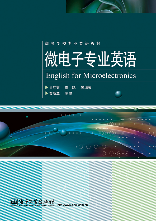
- 电子工业出版社
- 9787121177606
- 1-18
- 188008
- 48252897-3
- 平塑
- 16开
- 2024-04
- 770
- 336
- 工学
- 电子科学与技术
- TN4
- 电子科学与技术
- 本科 研究生及以上
目录
目 录
Session 1 Introduction to Semiconductor
1.1 What is Semiconductor
1.2 Classification of Semiconductor
Reading Materials
Session 2 Crystal Structure
2.1 Primitive Cell and Crystal Plane
2.2 Atomic Bonding
Reading Materials
Session 3 Band Model
3.1 Introduction to Quantum Mechanics
3.2 Band
3.3 Effective Mass Theory
Reading Materials
Session 4 The Semiconductor in Equilibrium
4.1 Charge Carriers in Semiconductor
4.2 Intrinsic Semiconductor
4.3 Extrinsic Semiconductor
Reading Materials
Session 5 Carrier Transport
5.1 Overview of Carrier Transport
5.2 Low Field Transport
5.3 High Field Transport
5.4 Diffusion Current
Session 6 Nonequilibrium Excess Carriers in Semiconductor
6.1 Recombination
6.2 Minority Carrier Lifetime
6.3 Ambipolar Transport
Reading Materials
Session 7 The pn Junction ( Ⅰ )
7.1 Introduction
7.2 Basic Structure of the pn Junction
7.3 Energy Bands for a pn Junction
7.4 Ideal CurrentVoltage Relationship
7.5 Characteristics of a Practical Diode
Reading Materials
Session 8 The pn Junction( Ⅱ )
8.1 Breakdown in pn Junction
8.2 SmallSignal Diffusion Resistance of the pn Junction
8.3 Junction Capacitance
8.4 Diffusion or Storage Capacitance
8.5 Diode Transients
8.6 Circuit Models for Junction Diodes
Reading Materials
Session 9 MetalSemiconductor Contacts
9.1 Schottky Contacts
9.2 Ohmic Contacts
Reading Materials
Session 10 Heterojunctions
10.1 Strain and Stress at Heterointerfaces
10.2 Heterojunction Materials
10.3 EnergyBand Diagrams
Reading Materials.
Session 11 The Bipolar Junction Transistor ( Ⅰ )
11.1 The Bipolar Junction Transistor Construction
11.2 Transistor Action
11.3 Nonideal Effects
11.4 Base Resistance
Reading Materials
Session 12 The Bipolar Junction Transistor ( Ⅱ )
12.1 Breakdown Voltage
12.2 Frequency Limits of BJT
12.3 The SchottkyClamped Transistor
12.4 Smallsignal Transistor Model
Reading Materials
Session 13 Basics of MOSFETs
13.1 Introduction
13.2 General Characteristics of a MOSFET
13.3 MOS System
13.4 Work Function Differences
13.5 FlatBand Voltage
13.6 Threshold Voltage
Reading Materials
Session 14 Nonideal Effects of MOSFETs
14.1 Introduction
14.2 Effective Mobility
14.3 Velocity Saturation
14.4 Channellength Modulation
14.5 DIBL
14.6 Hotcarrier Effect
14.7 GIDL
Reading Materials
Session 15 Advanced MOSFET Devices
15.1 Introduction
15.2 Channel Doping Profile
15.3 Gate Stack
15.4 Source/Drain Design
15.5 SchottkyBarrier Source/Drain
15.6 Raised Source/Drain
15.7 SOI
15.8 Three Dimensional Structure
Reading Materials
Session 16 Introduction to Integrated Circuits
16.1 Introduction
16.2 Size and Complexity of Integrated Circuits
16.3 Semiconductor Device for Integrated Circuits
16.4 IC Design Process
Reading Materials
Session 17 Analog Integrated Circuits Design
17.1 Introduction
17.2 Analog Signal Processing
17.3 CMOS Technology
17.4 Amplifiers
17.5 Differential Amplifiers
17.6 Operational Amplifiers
17.7 Characterization of Op Amps
Reading Materials
Session 18 Digital Integrated Circuits Design
18.1 Introduction
18.2 The Static CMOS Inverter
18.3 Designing Combinational Logic Gates in CMOS
Reading Materi


